(China (Mainland))

Product Summary
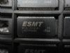
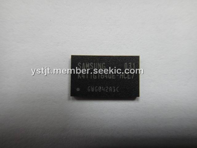
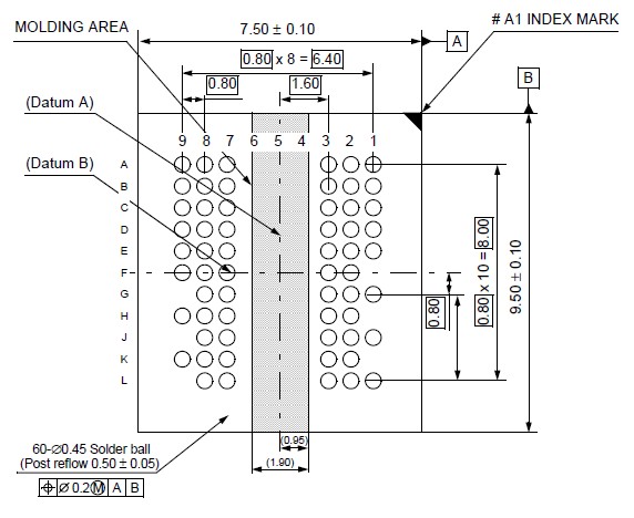
The 1Gb DDR2 SDRAM K4T1G164QE-HCE7 is organized as a 32Mbit x 4 I/Os x 8banks, 16Mbit x 8 I/Os x 8banks or 8Mbit x 16 I/Os x 8 banks device. This synchronous device K4T1G164QE-HCE7 achieves high speed double-data-rate transfer rates of up to 800Mb/sec/pin (DDR2-800) for general applications.
Parametrics
K4T1G164QE-HCE7 absolute maximum ratings: (1)Voltage on VDD pin relative to VSS:- 1.0V to 2.3V; (2)Voltage on VDDQ pin relative to VSS:- 0.5V to 2.3V ; (3)Voltage on VDDL pin relative to VSS:- 0.5V to 2.3V ; (4)Voltage on any pin relative to VSS:- 0.5V to 2.3V; (5)Storage Temperature:-55℃ to +100℃.
Features
K4T1G164QE-HCE7 features: (1)JEDEC standard VDD = 1.8V ± 0.1V Power Supply; (2)VDDQ = 1.8V ± 0.1V; (3)333MHz fCK for 667Mb/sec/pin, 400MHz fCK for 800Mb/sec/pin; (4)8 Banks ; (5)Posted CAS; (6)Programmable CAS Latency: 3, 4, 5, 6; (7)Programmable Additive Latenc y: 0, 1, 2, 3, 4, 5; (8)Write Latency(WL) = Read Latency(RL) -1; (9)Burst Length: 4 , 8(Interleave/nibble sequential); (10)Programmable Sequential / Interleave Burst Mode; (11)Bi-directional Differential Data-Strobe (Single-ended data strobe is an optional feature); (12)Off-Chip Driver(OCD) Impedance Adjustment ; (13)On Die Termination.
Diagrams
 |
 K4T1G044QA |
Other |
|
Data Sheet |
Negotiable |
|
||||
|
K4T1G044QM-ZCCC |
Other |
|
Data Sheet |
Negotiable |
|
||||
|
K4T1G044QM-ZCD5 |
Other |
|
Data Sheet |
Negotiable |
|
||||